- 您现在的位置:买卖IC网 > Sheet目录2008 > MAX1197ECM+TD (Maxim Integrated Products)IC ADC 8BIT 60MSPS DL 48-TQFP
MAX1197
Dual, 8-Bit, 60Msps, 3V, Low-Power ADC with
Internal Reference and Parallel Outputs
_______________________________________________________________________________________
3
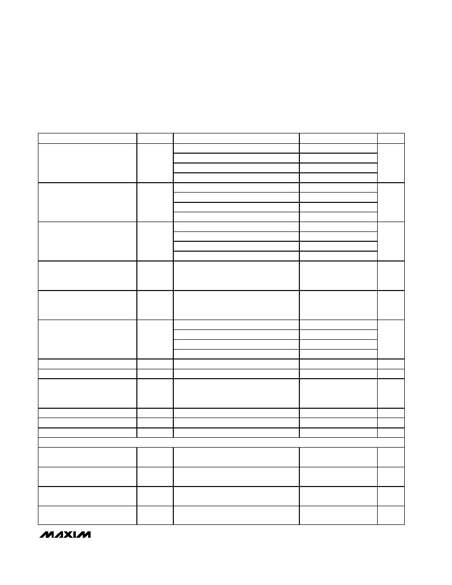
ELECTRICAL CHARACTERISTICS (continued)
(VDD = OVDD = 3V, 0.1F and 2.2F capacitors from REFP, REFN, and COM to GND; REFOUT connected to REFIN through a 10k
resistor, VIN = 2VP-P (differential with respect to COM), CL = 10pF at digital outputs, fCLK = 60MHz, TA = TMIN to TMAX, unless otherwise
noted.
≥ +25°C guaranteed by production test, < +25°C guaranteed by design and characterization. Typical values are at TA = +25°C.)
PARAMETER
SYMBOL
CONDITIONS
MIN
TYP
MAX
UNITS
fINA or B = 7.5MHz at -1dB FS
48.6
fINA or B = 20MHz at -1dB FS
46.5
48.6
fINA or B = 30MHz at -1dB FS
48.5
Signal-to-Noise
and Distortion
SINAD
fINA or B = 115.1MHz at -1dB FS
48.2
dB
fINA or B = 7.5MHz at -1dB FS
71
fINA or B = 20MHz at -1dB FS
60
69
fINA or B = 30MHz at -1dB FS
69
Spurious-Free
Dynamic Range
SFDR
fINA or B = 115.1MHz at -1dB FS
68
dBc
fINA or B = 7.5MHz at -1dB FS
-75
fINA or B = 20MHz at -1dB FS
-72
fINA or B = 30MHz at -1dB FS
-72
Third-Harmonic
Distortion
HD3
fINA or B = 115.1MHz at -1dB FS
-68
dBc
Intermodulation Distortion
(First Five Odd-Order IMDs)
IMD
fIN1(A or B) = 1.985MHz at -7dB FS
fIN2(A or B) = 2.029MHz at -7dB FS
(Note 2)
-70
dBc
Third-Order Intermodulation
Distortion
IM3
fIN1(A or B) = 1.985MHz at -7dB FS
fIN2(A or B) = 2.029MHz at -7dB FS
(Note 2)
-71.8
dBc
fINA or B = 7.5MHz at -1dB FS
-69
fINA or B = 20MHz at -1dB FS
-67
-57
fINA or B = 30MHz at -1dB FS
-67
Total Harmonic Distortion
(First Four Harmonics)
THD
fINA or B = 115.1MHz at -1dB FS
-65
dBc
Small-Signal Bandwidth
Input at -20dB FS, differential inputs
500
MHz
Full-Power Bandwidth
FPBW
Input at -1dB FS, differential inputs
400
MHz
Gain Flatness
(12MHz Spacing)
fIN1(A or B) = 106 MHz at -1dB FS
fIN2(A or B) = 118 MHz at -1dB FS
(Note 3)
0.05
dB
Aperture Delay
tAD
1ns
Aperture Jitter
tAJ
1dB SNR degradation at Nyquist
2
psRMS
Overdrive Recovery Time
For 1.5
× full-scale input
2
ns
INTERNAL REFERENCE (REFIN = REFOUT through 10k
resistor; REFP, REFN, and COM levels are generated internally.)
Reference Output Voltage
VREFOUT
(Note 4)
2.048
±3%
V
Positive Reference Output
Voltage
VREFP
(Note 5)
2.012
V
Negative Reference Output
Voltage
VREFN
(Note 5)
0.988
V
Common-Mode Level
VCOM
(Note 5)
VDD / 2
±0.1
V
发布紧急采购,3分钟左右您将得到回复。
相关PDF资料
MAX1202AEPP+
IC ADC 12BIT 8CH 20-DIP
MAX121EAP+
IC ADC 14BIT 308KSPS 20SSOP
MAX1238MEEE+T
IC ADC 12BIT SERIAL 16-QSOP
MAX1240AEPA+
IC ADC 12BIT SERIAL 8-DIP
MAX1245BCPP
IC ADC SRL 12BIT 2.375V 20-DIP
MAX1249AEPE+
IC ADC 10BIT SERIAL 16-DIP
MAX1279AETC+
IC ADC 12BIT 1.5MSPS 12-TQFN
MAX1285BESA+T
IC ADC 12BIT 300KSPS 8-SOIC
相关代理商/技术参数
MAX1197ECM-D
功能描述:模数转换器 - ADC RoHS:否 制造商:Texas Instruments 通道数量:2 结构:Sigma-Delta 转换速率:125 SPs to 8 KSPs 分辨率:24 bit 输入类型:Differential 信噪比:107 dB 接口类型:SPI 工作电源电压:1.7 V to 3.6 V, 2.7 V to 5.25 V 最大工作温度:+ 85 C 安装风格:SMD/SMT 封装 / 箱体:VQFN-32
MAX1197ECM-TD
功能描述:模数转换器 - ADC RoHS:否 制造商:Texas Instruments 通道数量:2 结构:Sigma-Delta 转换速率:125 SPs to 8 KSPs 分辨率:24 bit 输入类型:Differential 信噪比:107 dB 接口类型:SPI 工作电源电压:1.7 V to 3.6 V, 2.7 V to 5.25 V 最大工作温度:+ 85 C 安装风格:SMD/SMT 封装 / 箱体:VQFN-32
MAX1198E/D
功能描述:模数转换器 - ADC DICE SALES DICE RoHS:否 制造商:Texas Instruments 通道数量:2 结构:Sigma-Delta 转换速率:125 SPs to 8 KSPs 分辨率:24 bit 输入类型:Differential 信噪比:107 dB 接口类型:SPI 工作电源电压:1.7 V to 3.6 V, 2.7 V to 5.25 V 最大工作温度:+ 85 C 安装风格:SMD/SMT 封装 / 箱体:VQFN-32
MAX1198ECM+D
功能描述:模数转换器 - ADC 8-Bit 2Ch 100Msps 3.3V High Speed ADC RoHS:否 制造商:Texas Instruments 通道数量:2 结构:Sigma-Delta 转换速率:125 SPs to 8 KSPs 分辨率:24 bit 输入类型:Differential 信噪比:107 dB 接口类型:SPI 工作电源电压:1.7 V to 3.6 V, 2.7 V to 5.25 V 最大工作温度:+ 85 C 安装风格:SMD/SMT 封装 / 箱体:VQFN-32
MAX1198ECM+TD
功能描述:模数转换器 - ADC 8-Bit 2Ch 100Msps 3.3V High Speed ADC RoHS:否 制造商:Texas Instruments 通道数量:2 结构:Sigma-Delta 转换速率:125 SPs to 8 KSPs 分辨率:24 bit 输入类型:Differential 信噪比:107 dB 接口类型:SPI 工作电源电压:1.7 V to 3.6 V, 2.7 V to 5.25 V 最大工作温度:+ 85 C 安装风格:SMD/SMT 封装 / 箱体:VQFN-32
MAX1198ECM-D
功能描述:模数转换器 - ADC RoHS:否 制造商:Texas Instruments 通道数量:2 结构:Sigma-Delta 转换速率:125 SPs to 8 KSPs 分辨率:24 bit 输入类型:Differential 信噪比:107 dB 接口类型:SPI 工作电源电压:1.7 V to 3.6 V, 2.7 V to 5.25 V 最大工作温度:+ 85 C 安装风格:SMD/SMT 封装 / 箱体:VQFN-32
MAX1198ECM-TD
功能描述:模数转换器 - ADC RoHS:否 制造商:Texas Instruments 通道数量:2 结构:Sigma-Delta 转换速率:125 SPs to 8 KSPs 分辨率:24 bit 输入类型:Differential 信噪比:107 dB 接口类型:SPI 工作电源电压:1.7 V to 3.6 V, 2.7 V to 5.25 V 最大工作温度:+ 85 C 安装风格:SMD/SMT 封装 / 箱体:VQFN-32
MAX1198EVKIT
功能描述:数据转换 IC 开发工具 RoHS:否 制造商:Texas Instruments 产品:Demonstration Kits 类型:ADC 工具用于评估:ADS130E08 接口类型:SPI 工作电源电压:- 6 V to + 6 V